products categories
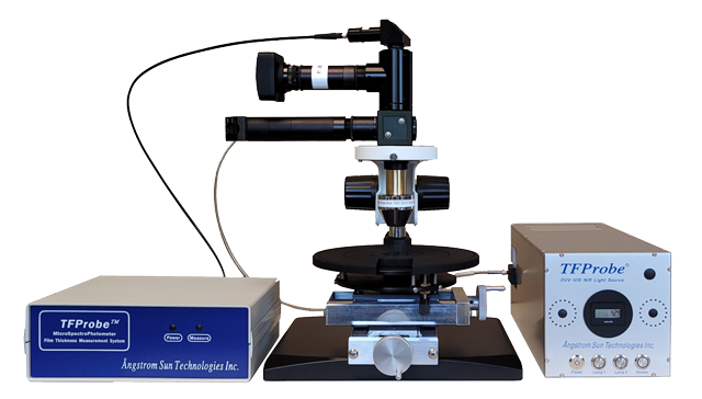
Angstrom Sun Technologies Inc just introduced an economical low cost micropsectrophotometer eMSP set of tools for micron region spectrum and film thickness measurement, it has the same wavelength coverage as regular/standard micropsectrophotometers, using the same TFProbe software for data acquisition, simulation, modeling and more... Its unique design ensures university and small startups to spend less money and get the same level characterizations for thin films.
Easy to operate with Window based software, both 32bit and 64bit OS
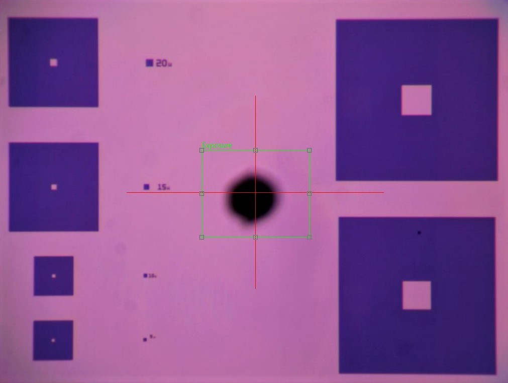
Micron region measurement with live video for patterned structure surface
Array based detector system to ensure fast measurement
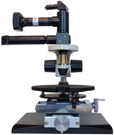
Affordable, portable and small footprint table top design
Measure film thickness and Refractive Index up to 5 layers over micron size region
Allow to acquire reflection, transmission and absorption spectra in milliseconds
Capable to be used for real time spectra, thickness, refractive index monitoring
System comes with comprehensive optical constants database and library
Advanced Software allows user to use either NK table, dispersion or composite model (EMA) for each individual film
Integrated Vision, spectrum, simulation, film thickness measurement system
Apply to many different type of substrates with different thickness up to 150mm size
User friendly data management interface
Imaging software for dimension measurement such as angle, distance, area, particle counting and more
Various options available to meet special applications
Model: eMSP100, eMSP300, eMSP400, eMSP450, eMSP500
Detector: CCD Array and/or InGaAs Array
Light Source: High Power Deutenium and/or Halogen lamp
Stage: Various Size with precision Z focus (fine and cause)
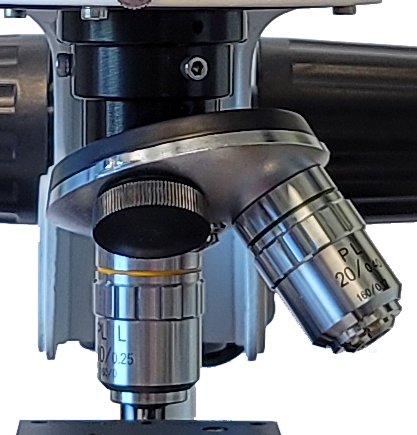
Objectives: available 4x, 10x, 20x, 40x, 50x
Communication: USB
Software: TFProbe 2.4 (upgradable to TFProbe 3.3)
Measurement Type: Reflection Spectra, Film thickness/refractive index and feature dimensions
Computer and Monitor: optional, both 32bit and 64bit OS
Power: 110– 240 VAC /50-60Hz, 3 A
Dimension: 20’x20’x20’ (Table top setup)
Warranty: One year labor and parts
Wavelgnth range: 200 to 1700nm (higher is also available)
Wavelgnth reolsution: typically <1nm for visible range and 3nm for NIR rnage
Spot Size: 10um (50x) and 50um (10x objective), other spot size is also available
Smaple Holder: 150x150mm
Substrate Thcikness: up to 50mm
Measurable thickness range*: 10nm to 100um or extended per specific configuration
Measurmeent time: minimum 2ms
Add-on accessories for Transmission Measurement
Wavelength extension to DUV (eMSP500)
Higher power optics for smaller spot size
Customized configuration for special applications
Heating and Cooling Stage for kinetics study
Higher wavelength resolution down to 0.1nm
Various filters for special applications
Precision X-Y stage
Semiconductor fabrication (PR, Oxide, Nitride..)
Liquid crystal display (ITO, PR, Cell gap…..)
Forensics, Biological films and materials
Inks, Mineralogy, Pigments, Toners
Pharmaceuticals, Medial Devices
Optical coatings, TiO2, SiO2, Ta2O5…..
Semiconductor compounds
Functional films in MEMS/MOEMS
Amorphous, nano and crystalline films
640nm SiO2on Silicon Sample
![]()
Native Oxide
![]()
Si3N4 Sample
![]()
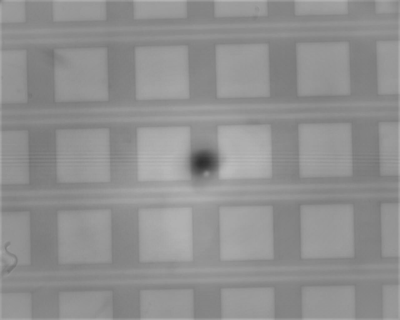
Digital Imaging Examples:
Note:
System configuration and Specifications subject to change without notice
* Film property, surface quality and layer stack dependent
Customized system available for special applications
TFProbe is registered trademark of Angstrom Sun Technologies Inc.

