products categories

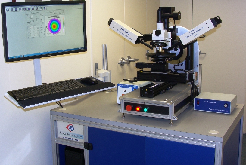
Angstrom Sun technolgies Inc provides a solution to work on ultra thin films with Ellipsometry and also a micron small area with micro-reflectometry, a unique configuration by combining ellipsometer and microspectrophtometers. TFProbe 3.3 version software will handle both measurements and analyses.
A small probing spot is desired for some applications, like features on MEMS or semiconductor product wafers. After microspectrophotometer is integrated with spectroscopic ellipsometer, tool's capability is greatly extended. Model SE-MSP is designed for such purpose. MSP works under reflectometry mode and run measuremment at normal incident angle which is complimentary to non-normal incident angle SE setup. Wavelength ranges for SE and MSP can be configured differently, based on application needs. All options are selectable.
- Easy to operate with Window based software
- Advanced optics design for best system performance
- Automatically change incident angles at 0.001 degree resolution with SExxxBA options
- High Power light source for broad band applications
- Array based detector system to ensure fast measurement
- Measure film thickness and Refractive Index for multiple layers, allow user to design model with unlimited layers
- System comes with comprehensive optical constants database and library
- Advanced TFProbe 3.3 Software allows user to use either NK table, dispersion (parameters) or effective media approximation (EMA) for each individual film.
- Three different user level control: Engineer mode, system service mode and easy user mode
- Flexible engineer mode for various recipe setup and optical model testing
- Robust one click button (Turn-key) solution for quick and routine measurement
- Configurable measurement parameters, user preference and easiness of operation
- Fully automatic calibration and initialization for system
- Precise sample alignment interface from sample signal directly, no external optics needed
- Precise height and tilting adjustment
- Apply to many different type of substrates with different thickness
- Various options, accessories available for special configurations such as mapping stage, wavelength extension, focus spot etc.
- 2D and 3D output graphics and user friendly data management interface
- Digital Imaging Tool for Micron region selection
- Integrated Reflectometer for Reflection measurement over small region
- Model: SE-MSP
- Detector: Detector Array
- Wavelngth range can be configured from 190 to 1700nm
- Light Source: Based on wavelength range for SE and MSP
- Incident Angle Change: Automatic with Program setting
- Stage: Manual or Automatic Mapping stage
- Software: TFProbe 3.3
- Combined SE and MSP
- Computer: Intel i3 processor
- Monitor: 22" Wide Screen LCD
- Power: Universal 110– 240 VAC /50-60Hz, 6 A
- Warranty: One year labor and parts
- Spot Size: 1 to 5 mm variable for SE (beam size can be reduced with microspot option)
- Incident Angle Range: 30 to 90 degree
- Incident Angle Change Resolution: 0.001 degree with automatic goniometer or 5 degree step with manual goniometer
- Digital Imaging: 1.3 MegPixels or better
- Effective Magnification: 1200x
- Long Work distance objective (12mm)
- MSP Beam Size: adjustable 10 - 500 um
- Sample Size: up to 300 mm in diameter
- Substrate Size: up to 20mm thick
- Measurable thickness range*: 0 nm to 50 µm
- Measurement Time: ~ 1s/Site
- Accuracy*: better than 0.25%
- Repeatability*: < 1 Å (1 sigma from 50 thickness readings for 1500 Å Thermal SiO2 on Si Wafer)
- Transmission Measurement Module
- High resolution digital camera
- Ultra Long work distance objective for MSP
- Mapping X-Y Stage (X-Y mode, instead of Rho-Theta mode)
- Heating /Cooling Stage
- Vertical Sample Mounting Goniometer
- Wavelength extension to further DUV or IR range
- Scanning Monochromator Setup
- Semiconductor fabrication (PR, Oxide, Nitride..)
- Liquid crystal display (ITO, PR, Cell gap…..)
- Forensics, Biological films and materials
- Inks, Mineralogy, Pigments, Toners
- Pharmaceuticals, Medial Devices
- Optical coatings, TiO2, SiO2, Ta2O5…..
- Semiconductor compounds
- Functional films in MEMS/MOEMS
- Amorphous, nano and crystalline Si
Note:
- System configuration and Specifications subject to change without notice
- * Film property, surface quality and layer stack dependent
- Customized system available for special applications
- TFProbe is registered trademark of Angstrom Sun Technologies Inc.

